Previously I did some posts about programming various AVR chips:
These three sketches have now been update to support "high-voltage" programming.
What is high-voltage programming?
Many of the AVR chips have multiple ways of programming them (changing the firmware on the Flash memory):
- Bootloader - this is the simplest, where code flashed onto the flash memory can detect that the flash needs reprogramming (typically from commands on the serial port) and reprograms the bulk of the flash. The bootloader is usually located in "high" memory, and the normal code starts at address zero.
- ICSP (In Circuit Serial Programming) - this uses six pins (RESET, MOSI, MISO, SCK, VCC, GND) to upload new code to the chip. This works by holding the /RESET pin low (zero volts) and then sending ICSP commands through the SPI pins. This can be used to upload code, change the fuses, and also to upload a bootloader.
- High-voltage Parallel programming - this uses a large number of pins (18) plus /RESET, VCC and GND. Using this method a "high voltage" (12 volts) is applied to /RESET which puts it into high-voltage parallel programming mode. It is called "parallel" because when sending data to the chip all 8 bits are read or written at once (in parallel).
- High-voltage Serial programming - this uses a small number of pins (4) plus /RESET, VCC and GND. Using this method a "high voltage" (12 volts) is applied to /RESET which puts it into high-voltage serial programming mode. It is called "serial" because data is sent to the chip serially (similar to SPI). One of the pins is SCI (serial clock input), one is SDI (data in to the chip), one is SII (instruction in to the chip), and one is SDO (data out from the chip). This method is suited to the smaller chips (like the ATtiny) which do not have enough pins for the high-voltage parallel programming.
So what is the use of the high-voltage programming? It lets you do things which are otherwise impossible. For example, you may have disabled SPI programming (ICSP programming). If you do that, then you can't reprogram the chip using ICSP. You may have also disabled the /RESET pin, freeing it up for use as an ordinary digital input/output pin. On a chip with only 8 pins this might be desirable. Using high-voltage programming you can recover from these situations, if you need to reprogram the chip, change the fuses, or change the lock bits.
Disadvantages
To use the high-voltage programming you almost certainly need to remove the chip from its circuit, and place it into a special programming jig. This is because normal circuits do not expect 12V on the /RESET pin, and probably have a pull-up resistor and/or a diode on /RESET. This would damage your chip or board if you try to apply 12 volts to reset whilst in circuit.
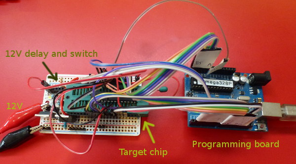
Programming jig - parallel programming
You basically just need a way of connecting up the 20 or so wires to the target chip. I soldered a zero insertion-force socket onto a breadboard, and then some header sockets next to it (the sockets like the ones on the Arduino Uno). On one end I also had some circuitry for switching on and off the 12V supply (discussed below).
The connections are documented in the source, reproduced here:
// Arduino pins                 Target pins
// ------------                 -----------------------
    6,                        // 14 (PB0) (data bit 0)
    7,                        // 15 (PB1) (data bit 1)
    8,                        // 16 (PB2) (data bit 2)
    9,                        // 17 (PB3) (data bit 3)
    10,                       // 18 (PB4) (data bit 4)
    11,                       // 19 (PB5) (data bit 5)
    12,                       // 23 (PC0) (data bit 6)
    13                        // 24 (PC1) (data bit 7)

      RDY     = A0,           //  3 (PD1) (low means busy)
      OE      = A1,           //  4 (PD2) (low means output enabled)
      WR      = A2,           //  5 (PD3) (low means write)
      BS1     = A3,           //  6 (PD4)
      XTAL1   = A4,           //  9 (XTAL1)
      XA0     = A5,           // 11 (PD5)
      XA1     =  2,           // 12 (PD6)
      PAGEL   =  3,           // 13 (PD7)
      BS2     =  4,           // 25 (PC2)
      VCC     =  5,           // 7 and 20 (VCC and AVCC)

 /RESET (pin 1) on target connected to 12V via a transistor and MOSFET as described below.
 Also connect the grounds. GND to pins 8 and 22.
 Decoupling capacitors: 0.1 µF (100 nF) between VCC/AVCC (pins 7 and 20) and Gnd.
 Not connected on target: pins 2, 10, 21, 26, 27, 28.
I tried to make the pins adjacent as much as possible, so you could use a ribbon cable to make the connections. Thus, for example, you connect D6 (Arduino digital pin 6) to pin 14 on the target.
This is for 28-pin targets like the ATmega8, ATmega48, ATmega88A, ATmega168, ATmega328.
Programming jig - serial programming
For serial programming of the smaller chips, you need a simpler setup, like this:

// Arduino pins                                  Target pins
// ------------                                  -------------------
    VCC   = 3,  // VCC                                      (pin 8)
    SDI   = 4,  // Serial Data Input                --> PB0 (pin 5)
    SII   = 5,  // Serial Instruction Input         --> PB1 (pin 6)
    SDO   = 6,  // Serial Data Output               --> PB2 (pin 7)
    SCI   = 7,  // Serial Clock Input (min. 220nS)  --> PB3 (pin 2)

 /RESET (pin 1) on target connected to 12V via a transistor and MOSFET as described below.
 Also connect the ground. GND to pin 4.
 Decoupling capacitor: 0.1 µF (100 nF) between VCC (pin 8) and Gnd.
 Not connected on target: pin 3.
This is for 8-pin targets like the ATtiny25, ATtiny45, ATtiny85.
Reset delay and switch
The /RESET pin needs to be brought to 12V between 20 to 60 µs after powering up the chip. In my case I had run out of spare pins to switch the 12V line directly, as I had used 18 out of the 20 pins on my Uno, and wanted to keep pins 0 and 1 free for serial communications. Thus I made up this circuit, which automatically switches 12V on about 30 µs after it is activated.

The RC network of R1/C1 reaches 0.7V after:
  t = - log ( (V - Vc) / V) * R * C

  -log ( (5 - 0.7)/5) * 22e3 * 10e-9 = 0.000033 seconds (33 µs)
For more details see Ladyada - RC Delay Calculator.
This turns on Q1 which shortly after turns on the MOSFET Q2 which switches 12V to the /RESET pin. Confirmed by the oscilloscope:

The delta time shown there is 48 µs which is about in the middle of the wanted range, for turning 12V on, within 20 to 60 µs after VCC reaches 1.8V.
Where do you get 12V from?
You need a separate supply of between 11.5V to 12.5V to activate the high-voltage programming.
I used a small 15W bench power supply, which happened to offer (amongst other things) regulated 12V output.
Another option could be a 12V wall-wart, however be careful that the output is regulated. Preferably measure with a meter before using it. For example, I have a so-called 12V plug-pack here:

However its output under no load was well over 12V:

That would not be suitable. It could be OK if you ran it through a voltage regulator, for example an LM7812 with appropriate capacitors:

Another approach would be to get the power supply module out of an old PC, and find the 12V supply pin. Google "pc power supply 12v" to find lots of articles about doing that.
Code
The code to implement the serial and parallel high-voltage programming has been incorporated into the following sketches:
- Atmega_Board_Detector (detects chip type, fuses and bootloader type)
- Atmega_Board_Programmer (installs a bootloader)
- Atmega_Hex_Uploader (erase chip, change fuse and lock bits)
Available from https://github.com/nickgammon/arduino_sketches
Note that near the start of these sketches are some defines that you need to set to get the appropriate programming type. Make one of them true.
// make true to use the high-voltage parallel wiring
#define HIGH_VOLTAGE_PARALLEL true
// make true to use the high-voltage serial wiring
#define HIGH_VOLTAGE_SERIAL false
// make true to use ICSP programming
#define ICSP_PROGRAMMING false
The defines above are currently set to do high-voltage parallel programming.
The code has been heavily reworked since previous versions. The main reason is that the code to program or read from the chips was duplicated in each sketch (basically, by copy-and-paste). This made updating very hard. Also the list of known chip signatures was duplicated between each sketch.
Now, the "shared" stuff is implemented in separate .ino and .h files. Whilst it might appear that there are still multiple copies of these files, on my disk (at least) the copies are just "soft links". For example:
lrwxrwxrwx 1 nick nick    38 May 27 07:15 General_Stuff.h -> ../Atmega_Hex_Uploader/General_Stuff.h
lrwxrwxrwx 1 nick nick    44 May 27 07:44 HV_Parallel_Utils.ino -> ../Atmega_Hex_Uploader/HV_Parallel_Utils.ino
lrwxrwxrwx 1 nick nick    32 May 27 07:16 HV_Pins.h -> ../Atmega_Hex_Uploader/HV_Pins.h
lrwxrwxrwx 1 nick nick    42 May 27 07:44 HV_Serial_Utils.ino -> ../Atmega_Hex_Uploader/HV_Serial_Utils.ino
lrwxrwxrwx 1 nick nick    37 May 27 07:44 ICSP_Utils.ino -> ../Atmega_Hex_Uploader/ICSP_Utils.ino
lrwxrwxrwx 1 nick nick    44 May 27 07:16 Programming_Utils.ino -> ../Atmega_Hex_Uploader/Programming_Utils.ino
lrwxrwxrwx 1 nick nick    35 May 27 07:16 Signatures.h -> ../Atmega_Hex_Uploader/Signatures.h
Because of this, if I change the file Signatures.h each of the sketches will now get the new copy.
[EDIT] Modified on 4 June 2015 to use hard links instead of soft links, because soft links were not working under Windows.
Example of installing a bootloader
Sketch: Atmega_Board_Programmer
Activating high-voltage PARALLEL programming mode.
Signature = 0x1E 0x95 0x0F
Processor = ATmega328P
Flash memory size = 32768 bytes.
LFuse = 0xFF
HFuse = 0xDE
EFuse = 0xFD
Lock byte = 0xEF
Clock calibration = 0x99
Type 'L' to use Lilypad (8 MHz) loader, or 'U' for Uno (16 MHz) loader ... U
Using Uno Optiboot 16 MHz loader.
Bootloader address = 0x7E00
Bootloader length = 512 bytes.
Type 'Q' to quit, 'V' to verify, or 'G' to program the chip with the bootloader ... G
Erasing chip ...
Writing bootloader ...
Committing page starting at 0x7E00
Committing page starting at 0x7E80
Committing page starting at 0x7F00
Committing page starting at 0x7F80
Written.
Verifying ...
No errors found.
Writing fuses ...
LFuse = 0xFF
HFuse = 0xDE
EFuse = 0xFD
Lock byte = 0xEF
Clock calibration = 0x99
Done.
Programming mode off.
Type 'C' when ready to continue with another chip ...
This takes around two seconds.
Example of the chip detector
Sketch: Atmega_Board_Detector
Atmega chip detector.
Written by Nick Gammon.
Version 1.16
Compiled on May 27 2015 at 13:55:02 with Arduino IDE 106.
Activating high-voltage PARALLEL programming mode.
Signature = 0x1E 0x95 0x0F
Processor = ATmega328P
Flash memory size = 32768 bytes.
LFuse = 0xFF
HFuse = 0xDE
EFuse = 0xFD
Lock byte = 0xEF
Clock calibration = 0x99
Bootloader in use: Yes
EEPROM preserved through erase: No
Watchdog timer always on: No
Bootloader is 512 bytes starting at 7E00

Bootloader:

7E00: 0x11 0x24 0x84 0xB7 0x14 0xBE 0x81 0xFF 0xF0 0xD0 0x85 0xE0 0x80 0x93 0x81 0x00
...
7FF0: 0xFF 0x27 0x09 0x94 0xFF 0xFF 0xFF 0xFF 0xFF 0xFF 0xFF 0xFF 0xFF 0xFF 0x04 0x04

MD5 sum of bootloader = 0xFB 0xF4 0x9B 0x7B 0x59 0x73 0x7F 0x65 0xE8 0xD0 0xF8 0xA5 0x08 0x12 0xE7 0x9F
Bootloader name: optiboot_atmega328

First 256 bytes of program memory:

0: 0xFF 0xFF 0xFF 0xFF 0xFF 0xFF 0xFF 0xFF 0xFF 0xFF 0xFF 0xFF 0xFF 0xFF 0xFF 0xFF
...
F0: 0xFF 0xFF 0xFF 0xFF 0xFF 0xFF 0xFF 0xFF 0xFF 0xFF 0xFF 0xFF 0xFF 0xFF 0xFF 0xFF

Programming mode off.
Example of changing fuses
Sketch: Atmega_Hex_Uploader
--------- Starting ---------

Activating high-voltage PARALLEL programming mode.
Signature = 0x1E 0x95 0x0F
Processor = ATmega328P
Flash memory size = 32768 bytes.
LFuse = 0xFF
HFuse = 0xDE
EFuse = 0xFD
Lock byte = 0xEF
Clock calibration = 0x99
Actions:
 [E] erase flash
 [F] modify fuses
Enter action: F
Programming mode off.
Activating high-voltage PARALLEL programming mode.
LFuse = 0xFF
HFuse = 0xDE
EFuse = 0xFD
Lock byte = 0xEF
Clock calibration = 0x99
Choose fuse (LOW/HIGH/EXT/LOCK) ... LOW
Current value of low fuse = 0xFF
Enter new value for low fuse (2 hex digits) ... D2
WARNING: Fuse changes may make the processor unresponsive.
Confirm change low fuse from 0xFF to 0xD2 . Type 'YES' to confirm ... YES
Activating high-voltage PARALLEL programming mode.
Changing low fuse ...
Fuse written.
LFuse = 0xD2
HFuse = 0xDE
EFuse = 0xFD
Lock byte = 0xEF
The hex uploader in this case can't actually upload any HEX files because there aren't any spare pins for connecting to the SD card. If you have a larger board (like the Mega2560) it should be possible to have the parallel programming, and upload .hex files in the same sketch. Make this define true to achieve that:
// make true if you have spare pins for the SD card interface
#define SD_CARD_ACTIVE false
Example of uploading a hex file
Sketch: Atmega_Hex_Uploader
--------- Starting ---------

Activating high-voltage SERIAL programming mode.
Signature = 0x1E 0x93 0x0B
Processor = ATtiny85
Flash memory size = 8192 bytes.
LFuse = 0xF1
HFuse = 0xDF
EFuse = 0xFE
Lock byte = 0xFF
Clock calibration = 0xA4
Actions:
 [E] erase flash
 [F] modify fuses
 [L] list directory
 [R] read from flash (save to disk)
 [V] verify flash (compare to disk)
 [W] write to flash (read from disk)
Enter action: W
Programming mode off.

Activating high-voltage SERIAL programming mode.

Choose disk file [ FIRMWARE.HEX ] ... MICRON~1.HEX

Processing file: MICRON~1.HEX
Checking file ...

###
Lowest address  = 0x0
Highest address = 0x1FD7
Bytes to write  = 1824
No bootloader fuse.
Activating high-voltage SERIAL programming mode.
Processing file: MICRON~1.HEX
Erasing chip ...
Writing flash ...

##############################
Written.
Processing file: MICRON~1.HEX
Verifying flash ...

#############################
No errors found.
No bootloader fuse.
This was done with an ATtiny85, because that uses high-voltage serial programming, and therefore there were spare pins for the SD card interface (the SPI pins). |